Circuit Diagram Of Forward Bias Reverse Bias Circuit Diagram
Reverse biasing forward circuit between difference bias definition current differences key barrier potential Solved circuit diagram: m fig. 1: forward bias condition Zener diode characteristics
Study of forward and reverse characteristics of a pn junction diode.
Diode bias junction circuits Difference between forward & reverse biasing with comparison chart Pn junction diode: forward and reverse bias characteristics
Biasing difference bias diode voltage
Circuit diagram: a) forward bias: (0-200 ma 1 κω wDifference between forward & reverse biasing with comparison chart What is forward bias and reverse bias? example, applicationsStudy of forward and reverse characteristics of a pn junction diode..
Forward biasing of pn junction diodeBiased diode bias diodes Zener diode reverse bias circuit diagramSemiconductor diode.

Reverse bias circuit diagram
Schematic diagram of samples and series circuit under forward bias (aForward bias, reverse bias and their effects on diodes Forward bias & reverse bias diode working animationForward biasing of pn junction diode.
Diode junction pn forward bias characteristics circuit reverse biasing voltmeter ammeter plot assumeForward and reverse bias circuit diagram Schematic diagram of samples and series circuit under forward bias (aBias forward reverse diode biased rectifiers.

Circuit wiring diagram xii circuit diagrams pn junction forward bias
Diode bias forward animation working reverse gif instrumentationtoolsSemiconductor diode forward bias Diode junction characteristics semiconductor potential barrier emittingA forward bias circuit arrangement with two dc supply.
Junction forward bias curve characteristic diode biasedReverse bias circuit diagram Forward bias circuit diagram 26567194 vector art at vecteezy[get 22+] schematic diagram of junction diode.

Forward and reverse bias circuit diagram
Bias biasing pn diode junction etechnog transistors barrierTo draw the i-v characteristic curve of a p-n junction in forward bias Pn junction diode and vi characteristics » pija educationForward bias circuit diagram.
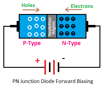
What is forward bias of pn junction diode?☑ forward biased diode circuit Rectifiers, forward bias and reverse biasPn junction forward bias circuit diagram.

Forward biased circuit diagram
☑ diode zero biasPn junction diode and its forward bias & reverse bias characteristics .
.

Study of forward and reverse characteristics of a pn junction diode.

a Forward bias circuit arrangement with two dc supply | Download

Circuit Wiring Diagram Xii Circuit Diagrams Pn Junction Forward Bias

Forward And Reverse Bias Circuit Diagram

Forward Biased Circuit Diagram

☑ Diode Zero Bias
![[Get 22+] Schematic Diagram Of Junction Diode](https://i2.wp.com/www.electronics-tutorials.ws/wp-content/uploads/2018/05/diode-diode7.gif)
[Get 22+] Schematic Diagram Of Junction Diode